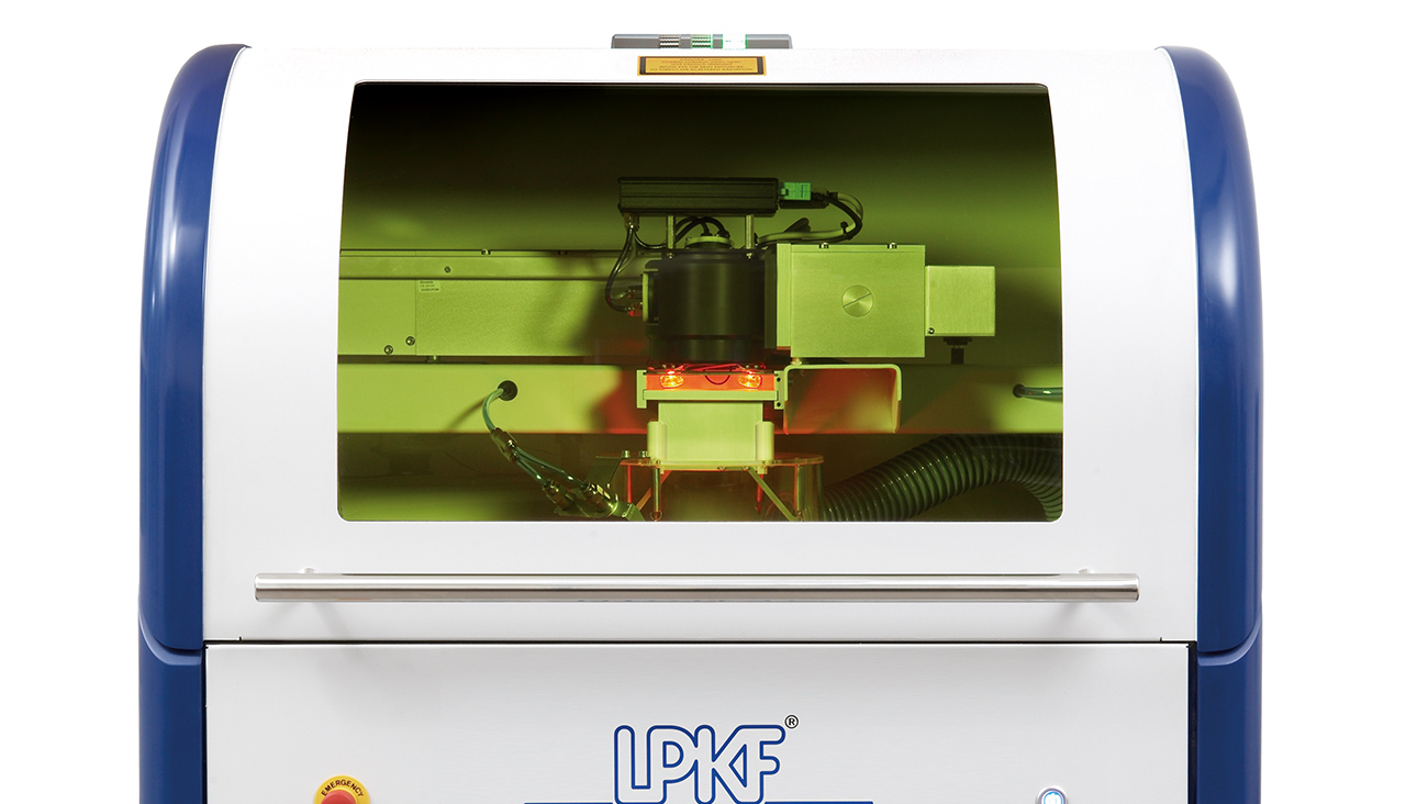
Fraunhofer Institute Flies through Material Trials of Millimeter-wave Circuits with a ProtoLaser S
Challenge:
Hoping to explore the region further, Germany’s Fraunhofer Institute for Applied Solid State Physics, named after Joseph von Fraunhofer who investigated the properties of visible light as early as 1820, has enlisted the aid of a ProtoLaser S system from LPKF Laser & Electronics for rapid fabrication of prototype circuits on a wide range of printed-circuit-board (PCB) materials. The Fraunhofer Institute is involved in not only engineering new solutions for millimeter-wave devices and components, but in enabling their use in practical applications.
For example, high-frequency radiometers can be used to continuously measure the temperature and humidity of the atmosphere using a ground-based system. Millimeter-wave circuits are also used in radar, in airport body scanners, in industrial metrology, safety engineering, astronomy, and in environmental surveys. In order to explore the commercial deployment of its millimeter-wave developments, the Fraunhofer Institute needed the means of fabricating fine-featured circuits from a variety of different PCB substrate materials. The ProtoLaser S system from LPKF uses high-energy pulsed laser beams to selectively ablate the conductive layer (usually copper) of a PCB laminate to form the thin transmission lines and circuit structures needed in support of millimeter-wave frequencies.
Solution:
A compact, laboratory-qualified laser system designed specifically for prototyping as well as on-demand small batch production of PCBs are equipped with casters for mobility and requires only compressed air, a vacuum, and a standard 110-VAC power outlet. Using a patented process, the laser can structure circuitry with great precision on most circuit substrates. The laser beam circumscribes the contours of circuit artwork on fully clad PCB material, thus producing the wiring structure. The laser system can process circuit layouts as large as 229 x 305 mm with a structuring speed of about 1-2 per minute (6 cm2 per minute). It works with flexible and rigid substrate materials, including copper-coated FR-4, polytetrafluoroethylene (PTFE), and ceramic substrates. The contact-free process results in handling sensitive materials without damage, resulting in high yields. The best precision is when using ceramic materials. On ceramic materials, the conductive layer is vaporized, allowing for conductor tracks with a width of only 50 μm (0.002 in.) and spacing as small as 25 μm (0.001 in.). Process parameters can be stored in memory for future research or small production runs.
The ProtoLaser incorporates an internal forced-air cooling system for long-term reliability. The system measures 34.5 x 56.3 x 29.5 in. (875 x 1430 x 750 mm) and weighs 573 lbs. (260 kg). The Fraunhofer Institute has used the ProtoLaser S system to fabricate circuits for millimeter-wave applications, such as this four-channel IF amplifier for 94-GHz radar modules, which are produced quickly. The system has also been used to produce a 15-GHz voltage controlled-oscillator (VCO) circuit for a multiplexer that generates signals in the 90-GHz range. This 15-GHz VCO was optimized using the ProtoLaser S system to fabricate different circuits, including a test board and finished circuit.
Results:
Engineer Michael Kuri, one of the specialists at the Fraunhofer Institute on combining RF semiconductors with circuit carrier systems says, "Having the ProtoLaser S system on site at the Fraunhofer Institute allows its engineers to react quickly when modifications to a design are needed. For example, the development of a slot antenna for an innovative radar system. The antenna required virtually radii-free cutouts in order to achieve the radiation properties needed for the radar system. The production time to produce the antenna with previous machining services and methods was three days or more; with the ProtoLaser S system, this was reduced to two minutes."


